The Serial Synchronous Interface
The SSI interface seems very similar, if not identical, to an SPI interface:
- Chip Select. On the AS5040, this is pin 11 and labelled 'CSn'. The line is normally high but is
taken low by the microcontroller whenever communication between the Picaxe and the AS5040 is required. CSn has an internal pull-up.
- Clock. This is provided by the Picaxe and enables data transfers to keep synchronized. On the AS5040, this is an input on pin 10.
It's a standard CMOS logic input.
- Data Out from the AS5040 to the Picaxe. Equivalent to MISO (Master In, Slave Out) on the SPI interface. The AS5040 calls
this signal 'DO' and is available on pin 9. When the CSn line is high, the
data line is in its high impedance (tri-stated) configuration so the Picaxe input should have its normal 10k resistor to ground.
Page 10 in the AS5040 datasheet shows the SSI timing and isn't as daunting as it first appears. This diagram shows a simplified version:
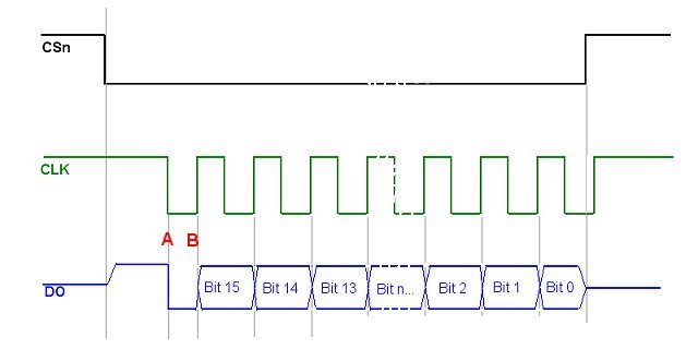
When the Chip Select CSn line is high, it doesn't really matter what the CLK line does. The Data Out line (DO) will be tri-stated. This allows other SSI devices to share the same SSI bus.
As soon as CSn is taken low, the Data Out line comes out of hibernation and assumes a normal CMOS logic high. After a small delay (500nS), the next falling edge of the CLK line will cause the AS5040 to load its internal register with data (Point A on the diagram above). The Data Out line falls to logic low but, at this time does not contain valid data.
At the first rising edge of the CLK (Point B), the first bit of the data (Bit 15) will be put on the data line, DO. It's up to the Picaxe to read whether the data line is high or low at this moment and use it to start assembling a 16-bit 'word'.
At subsequent rising edges of the CLK line, successive bits will be put on the DO line, for the Picaxe input to read, until all 16 bits have been communicated. The CSn line is again taken high and the DO line will be tri-stated.
Only the 10 Most significant bits (the first 10 to be sent) contain rotational (bearing) information (as a 0 to 1023 value). The remaining bits contain status information, such as the state of the 'MAG inc' and 'MAG dec' pins. This data can be useful to indicate the validity of the bearing information but the program below doesn't take them into account.
    	Symbol DataIn = w0		;DataIn will hold 16 bits from AS5040
    	Symbol BitCount = b2		;Bit counter
    	Symbol CSn = B.1		;AS5040 Chip Select (active low)
    	Symbol CLK = B.2		;AS5040 Clock input from Picaxe
    	Symbol DOut = pinC.2		;AS5040 Data Out  to Picaxe C.2 (MISO)

    	high CSn			;Chip not selected
    	high CLK			;Clock to idle

  	do
    	  DataIn = 0 			;Clear data bits
    	  low CSn			;Enable AS5040 chip select
          low CLK			;Pre-load internal AS5040 register
    	  for BitCount = 1 to 16	;Clock in 16 bits
      	     high CLK			;AS5040 puts bit on DOut
      	     DataIn = DataIn * 2 + DOut	;Shift DataIn bits to left and add new bit.
      	     low CLK			;
    	  next
    	  high CSn			;16 bits in so disable Chip Select
	  high CLK			;Make CLK high so it is ready for next falling edge
    	  DataIn = DataIn / 64		;6 LSB are AS5040 status bits so
    					;Shift 10 data bits to right (6 times)
    	  debug				;'debug' to examine data in Prog/Ed
    	  pause 100
  	loop
Analogue & SSI Compared
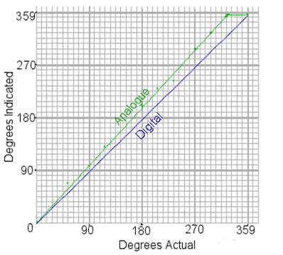
The AS5040 is extremely sensitive to variations in the magnetic field as the magnet is rotated above it. To give a fair trial to both analogue and SSI readings, I had to hold the breadboard in place with a small wooden jig with a "bridge" over the centre of the chip so that the magnet could be rotated accurately and smoothly. I'm currently designing/building the mechanical housing for an AS5040 project so will be able to provide more accurate angular readings then.The correlation between the actual angle turned and the displayed value is critically dependent on the positioning of the magnet above the chip. To all intents and purposes, the SSI output closely followed the actual angle turned. The analogue values showed increasing error as the angle increased. The error is consistent, though, so it should be easy to add in a factor (except for the "dead spot" after 330 degrees). Other factors, such as the distance between the AS5040 and the Picaxe would obviously affect the accuracy of the analogue signal - depending where the RC filter circuit is located.
 |  |
The following Picaxe program reads the analogue signal derived from the PWM output and the SSI signal and displays both on an LCD.
	; Austria Microsystems AS5040 Magnetic Rotary Encoder

	  Symbol DataIn = w0			;DataIn will hold 16 bits from AS5040
	  Symbol BitCount = b2			;Bit counter
	  Symbol CSn = B.1			;AS5040 Chip Select (active low)
	  Symbol CLK = B.2			;AS5040 Clock inut from Picaxe
	  Symbol DOut = pinC.2			;AS5040 Data Out  (MISO)

	  Symbol SSIDegrees = w3		;Raw output converted to degrees
	  Symbol AnalogDeg = w4


	init:
  	  high CSn				;Chip not selected
 	  low CLK				;Clock to idle
  	  pause 100

  	  hsersetup B9600_4, %10000 		;Use LCD Pin 1, no hserin


 	  hserout 0, (13) : pause 100           ;Initialize LCD
  	  hserout 0, (13) : pause 100
 	  hserout 0, (13) : pause 100
 	  pause 500
  	  hserout 0, ("ac1", 13)  		;Clear display
  	  pause 50
  	  hserout 0, ("acc", 13)                ;Hide cursor

	do

  	  ;================================
  	  ;READ ANALOGUE FROM PWM
  	  ;================================

 	  readadc10 C.1, AnalogDeg
 	  AnalogDeg = AnalogDeg * 64 / 182
  	  hserout 0, ("ac80", 13)
  	  hserout 0, ("adAnalogue: ", #AnalogDeg, "   ", 13)
  	  pause 100

  	  ;=================================
  	  ;SSI
  	  ;=================================

  	  DataIn = 0 				;Clear data bits
  	  low CSn				;Enable AS5040 chip select
	  low CLK				;Tell AS5040 to pre-load its data register
  	  for BitCount = 1 to 16		;Clock in 16 bits
    	     high CLK				;AS5040 puts bit on DOut
    	     DataIn = DataIn * 2 + DOut		;Shift DataIn bits to left and add new bit.
    	     low CLK				;
  	  next
  	  high CSn				;16 bits in so disable Chip Select
	  high CLK				;Make CLK high so it is ready for next falling edge
  	  DataIn = DataIn / 64			;Bit 0 to Bit 5 are AS5040 status bits so
 						;Shift 10 MSB data bits to right (6 times)

  	  SSIDegrees = DataIn * 64 / 182	;Convert 0 - 1023 to 0 - 359. There's
  						;an obvious maths shortcut there!

  	  debug

  	  hserout 0, ("acc0", 13)
  	  hserout 0, ("adSSI:      ", #SSIDegrees, "   ", 13)
  	  pause 100

	loop