Designing the Printed Circuit Board
|
Once you've collected the components, you're ready to begin designing the printed circuit board (PCB). It's
difficult to design the board sooner unless the supplier's catalogue or website gives exact dimensions of
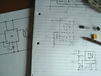
the components. For most components, you'll also need to know which pin is which - the "pinout". This information is usually available in the supplier's catalogue or on their website. If not, a Google search will generally find the information you need. Obviously, you need look no further than this tutorial for the pinouts of the components we're using here. Once armed with the necessary information, we can begin making rough pencil sketches of the components as we'll lay them out on the board with their inter-connecting copper tracks. |
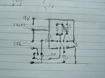
Remember that the tracks cannot cross. You may need to stop the track and use a wire jumper on the other side of the board. Try to keep such jumpers to a minimum because it'll mean less soldering to do but, at the same time, don't be afraid to use one if the path taken by the track would otherwise be too complicated. Our simple rub-down etch-resist transfers need simple, short, straight tracks wherever possible.
|
Take your time designing the layout, double-checking against the circuit diagram at regular intervals.
There's nothing more annoying than finding an error in the layout once the board is finished. It's up
to you how neat you make this final drawing because you now need to copy it onto a piece of printed
circuit board. With a simple circuit, you may be able to copy it by eye. With a more compicated circuit, you may need to trace it through with carbon paper - in which case, the pencil drawing would need to be exact. It's difficult to give specific advice when laying out the circuit - just take your time and don't try to cramp everything into too small a space. |
|
|
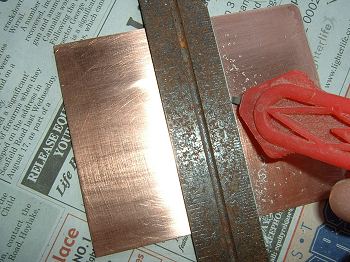
Once you're happy with the layout, cut a piece of printed circuit board to the correct size. I use a tile
cutter. Score deeply through the copper until you're about halfway through the board. Turn it over and
score the plain side. Fibreglass board is pretty tough so you need to score quite deeply but then it
should snap cleanly. Clean up the edges and remove the sharp edge from the copper where you scored it. Besides being a safety hazard - copper cuts are particularly prone to infection - a sharp edge can be a nuisance when you're using the rub-down transfers. Finally, give the copper surface a good clean with fine sandpaper to remove the oxide coating which inevitably forms. This coating will prevent the transfers from sticking properly and will slow down the etch process and cause uneven etching. |