Once the layout has been decided, cut a piece of printed circuit board to size by scoring a line
on both sides using an old tile cutter. Score completely through the copper on the copper side and at least deep enough to break through the top surface on the non-copper side. It
should then break cleanly on the line.
Clean and roughen the surface thoroughly using very fine sandpaper to remove the oxide coating which forms. This coating prevents the etch-resist transfers sticking properly and resists the etching processes itself thus slowing the process down and producing uneven etching.
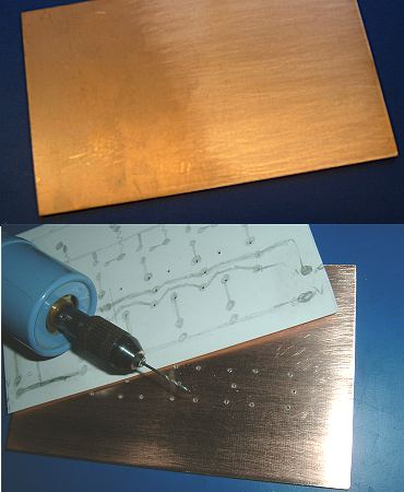
Once the board is clean, temporarily attach the card template to the copper side and drill through the holes which were previously made in the template to mark those components which required accurate positioning.
I use a 12v hand-held modelling drill and a 0.75mm drill bit. For some components with thin wires, a 0.5mm drill bit would be sufficient whilst others may require up to 1mm.