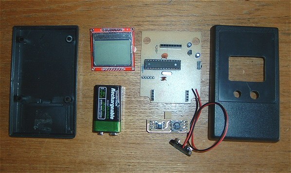
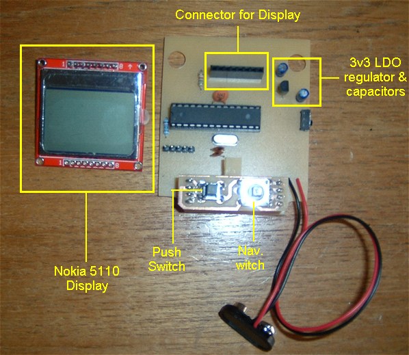
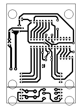
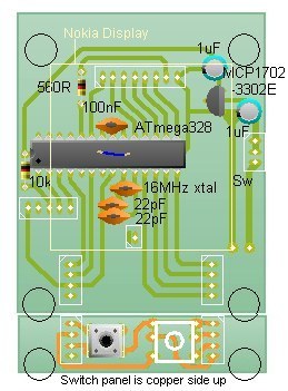
The Printed Circuit Board
There are a few different pin arrangements on the Nokia 5110 display so the PCB may need a bit of modifying, especially the connection to the LED backlight, which requires the 560R series resistor, and the Ground. All the other pin designations (including Vcc) can be determined in the software.The main PCB and the switch panel PCB can be etched together but the switch panel needs trimming afterwards to clear the enclosure's internal plastic pillars.
The PCB artwork in Circuit Wizard format can be downloaded here together with the Arduino sketch.
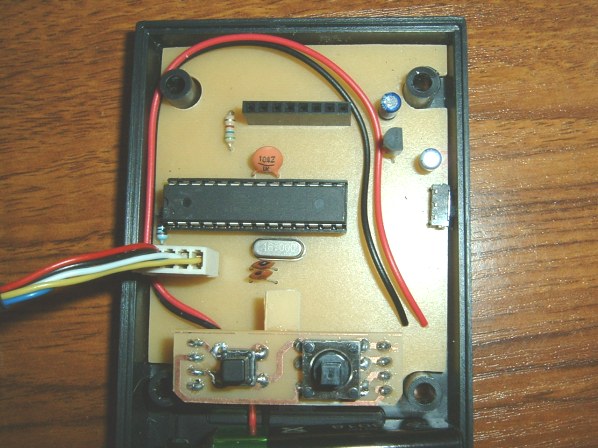
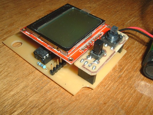
Assembly
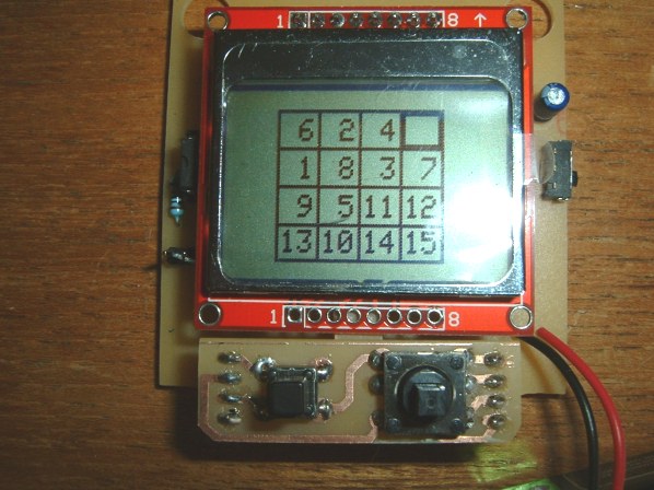
This photo shows the components soldered to the PCB and switch panel. Note the small 'tab' of PCB material super-glued to the underside of the switch panel to act as a support for the bottom edge of the Nokia display.Note that the switch panel is designed copper side up to allow the 4-way pin headers at each end to be inserted from underneath and soldered on the top side. There's enough of the tactile switch pins accessible on the top side to allow for soldering.