The Switching Circuit PCB
 The Maxim MAX3412 is only available as a Surface Mount Device (SMD) and, as this was to be a prototype project,
I looked for a way to install the chip using a socket. Although Maxim recommend that you don't use a socket,
I have very little experience of handling SMDs and even less in a design/prototype situation.
The Maxim MAX3412 is only available as a Surface Mount Device (SMD) and, as this was to be a prototype project,
I looked for a way to install the chip using a socket. Although Maxim recommend that you don't use a socket,
I have very little experience of handling SMDs and even less in a design/prototype situation.Maybe I'll practice soldering SMDs myself one day but, as this project is to be designed from scratch, having the option to use an IC socket seemed preferable.
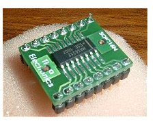
Fortunately, a company called "Tirna Electronics" makes a suitable adaptor. Even better, this company will source the device (from RS Components) and solder it to the adaptor, complete with a high quality 16-pin header.
Even with the adaptor plugged into an IC socket, the quality of the video is excellent.
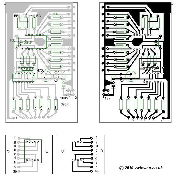 This is the layout I used for the printed circuit board. Please note that this is hand-drawn using a standard paint program so it's important that
you check out the pin spacing of the components yourself rather than copying this layout verbatim.
This is the layout I used for the printed circuit board. Please note that this is hand-drawn using a standard paint program so it's important that
you check out the pin spacing of the components yourself rather than copying this layout verbatim.
Click here for a larger layout view
If you design your own, bear in mind that Maxim recommend extending the ground plane as much as possible except around pins 15 & 16 and the output gain-control resistors, RF and RG.
The smaller PCB is for the 7-segment LED which is attached to the front panel of the case.
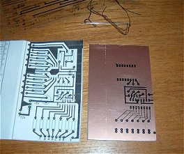
I made the PCBs using rub down etch resist transfers. In the following images, you'll notice deviations from the layout design because changing the route of the tracks made life easier when I came to actually apply the transfers.
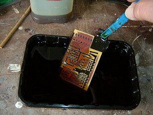 Etching the PCB (in the garage!) | 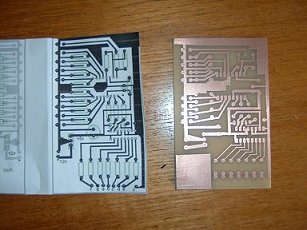
Completed PCB before drilling | 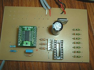 Top side. Note the 75Ω resistors are not fitted. |
Points to note
With this particualar PCB layout, please note:The two IC's orientation is NOT the same (the square dot denotes pin 1).
Note the 5-pin header near the socket for the 4511B. The outer pins carry 0v and +5v. These pins will supply power to the switching and timing board. (0v is also the common ground for the data lines). Because of the layout of the PCB (and the pin-out of the two ICs), data pins D1 and D2 are reversed on this header. Therefore, counting from the outer edge of the board towards the large capacitor, the pins are 0v, D0, D2, D1, +5v.
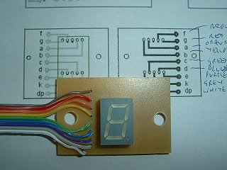 |  |
The far photograph shows the seven-segment LED display board prior to attaching it to the case. The near photo
shows initial testing. For convenience, I'm using a Velleman USB Experimenter's board (in the foreground) to provide
the data lines to the 5-pin header. In the finished project, the header will connect to a miniature 4-pin socket on the back of the case or to the 'Data Out' header on the automated switching and timing board if it is used. |
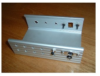 The image to the left shows the case I used for the project. Maplins used to supply this case but have stopped stocking it. Similar
Maplin cases do not have a removable bottom (or top) which makes them virtually impossible to use for a project like this.
The image to the left shows the case I used for the project. Maplins used to supply this case but have stopped stocking it. Similar
Maplin cases do not have a removable bottom (or top) which makes them virtually impossible to use for a project like this.
Top right of the photo shows the cut-out for the 7-segment display. I chain-drilled and filed to get the rectangular shape. Note the two bolts Araldited onto the case to provide 'studs' for the display board. A simpler solution would be to just drill a couple of holes through the case!
Because the inside of the case has grooves to hold the PCBs, mounting the LED display behind the rectangular hole would have resulted in the untidy-looking edges of the hole being on show. Making the display a 'neat' fit in the hole and fitting it flush with the front, concealed the untidy edges.
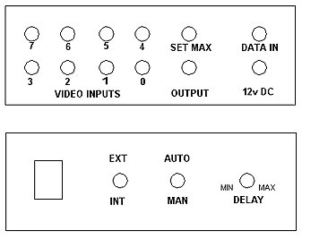
The 8 holes at the bottom left (the back of the case) are for the 8 phono sockets for the video inputs. There are two sockets at the right hand end of the back. The top one is a miniature 4-pin socket for the three incoming data lines (plus ground) from the computer parallel port, Velleman USB board, etc. The bottom socket is for the 12v DC power in.
Near the centre of the back panel, hidden from view by a push button switch, is a hole for the video out phono socket. The push button plays a part in the switching and timing circuit, to be discussed on the next page...
 Drilling details for the case. | 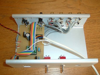 This photo shows the first part of the project more-or-less completed. All the phono sockets have been connected using screened cable. The data lines are still connected to the temporary Velleman testing board and the 12v DC and 4-pin external data sockets still need to be wired up. I've left enough 'slack' in the screened cables to the phono sockets to allow the PCB to be partially slid out of its mounting grooves. This will allow the fitting of any 75 ohm resistors or changes to the RF/RG gain control resistors if it should become necessary. I've also provided a 'loop' of slack in the red and black twisted pair to the 12v DC input socket. |