Module 2: The switching and timing circuit
This second part of the video switcher allows control of the three video selection data lines to be swapped from the external source (parallel port, Velleman USB board, etc) to internal control. This internal control needs to provide the following functions:- Automatically increment the video sources with an adjustable delay between each.
- Ability to set the highest available video source so the controller doesn't sequence through blank inputs.
- Manual selection of any video source.
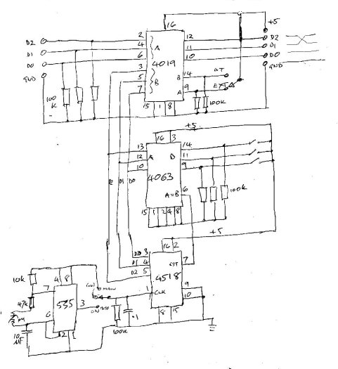
I initially designed a circuit using 4000-series CMOS ICs and a 555 timer. While I was struggling to design the PCB layout, it ocurred to me that a PIC® Microcontroller might be ideally suited. It was nearly 11 years since I'd last looked at these chips and, to be honest, I'd been put off by the comparative difficulty in programming the things. Between the programming hardware, the programming software and the final project board, there always seemed to be a chicken and egg situation with a few too many simultaneous learning curves - at least for me!
Although they've been around for something like 10 years, I've only recently become aware of a "spin-off" technology called PICAXE® from Revolution Education Ltd. These microchips start off as "ordinary" PIC® Microcontrollers but with the programming and code-execution software already programmed in as a sort of "bootstrap loader" or "BIOS". They can be programmed in situ on the finished project's board by the simple provision of a 3.5mm stereo socket and a couple of resistors. This means they can be programmed and re-programmed with different software without having to remove them from the project. Once the chip's safely in its socket with no bent pins, it can stay there!
The company provides free programming/editing software and free support. This was the perfect opportunity to give them a try!
(For anyone interested in the original CMOS design, you'll find a very rough UNTRIED diagram, here).
The PICAXE Circuit
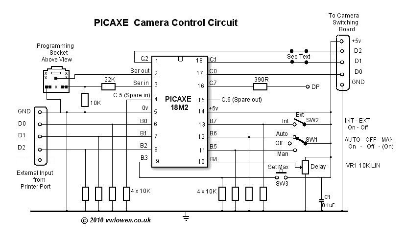
Operation of the circuit is controlled by the software we download into the PICAXE chip through the programming socket (shown at top left in the diagram above). Once programmed, the software remains in the chip even if the supply is removed and later restored.
The three data lines, D0, D1 and D2, on the left of the diagram are the three external lines from the computer's parallel port or the Velleman USB board. They are connected to three of the chip's pins which the chip automatically defaults to be inputs at power-up (B.0, B.1 and B.2). If switch SW2 is open (External), the three data lines are simply passed through the chip and appear on its output pins at C.0, C.1 and C.2. (Our software will configure these pins as outputs). From there, they simply connect via a couple of headers to the data input of the Video switching board. To all intents and purposes, this second circuit is effectively 'transparent.'
When SW2 is closed (Internal), the data lines at B.0, B.1 and B.2 are ignored and control of the output pins (C.0, C.1 and C.2) passes to the software inside the PICAXE itself:
- With SW1 set to 'Off', the progarm simply loops doing nothing. Whichever output pins were active when SW1 was set to 'Off'
will remain active indefinitely. That is, the selected video source won't change.
- With SW1 set to 'Auto', the program will increment the BCD count at the output pins - thus incrementing the selected
video source. The time between each increment is controlled by changing the voltage at the analogue input, B4. A delay anywhere between 10 and 60 seconds
is available but the range of times can easily be changed in the software.The output on C.7 is used to light the decimal point on the display when 'Auto' is selected.
Left to its own devices, the software will cycle through 0 to 7 and then start at 0 again. Unless all eight inputs are used, this is unsatisfactory because we could be left with several minutes of blank video while the unit cycles through the unused inputs. We can stop this happening by telling the PICAXE chip how many cameras we have installed by switching SW1 to the 'Manual' position...
- The 'Manual' position of SW1 is biased towards 'Off' so we need to hold the switch in the manual position. In this
position, the software will cycle quite rapidly through all the video inputs (0 - 7) and we can stop it at any position by releasing the
switch. Unused video inputs are scanned through in less than a second or two so are not a problem.
If we select the last occupied video input with the manual switch and then momentarily press the normally open push button (SW3), the number of this input will be stored in the chip and remembered - even through a power cycle. When SW2 is next put to 'Auto', it will only cycle round up to this input number.