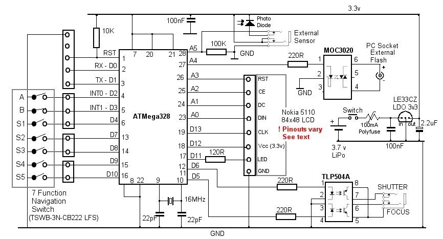
The Circuit
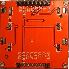
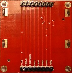
The Navigation Switch
The Camera Controller is configured using a 7-function Navigation Switch. Tactile buttons for up, down, left and right are used, primarily, to navigate the options on an LCD screen and the central 'OK' button selects the chosen option.Additionally, the switch has a 12 pulse/360° rotary encoder. This is used for instant access to the photodiode's sensitivity adjustment (or anything plugged into the external sensor socket) making it unnecessary to negotiate the configuration menus to adjust the sensitivity quickly.
The tactile buttons are connected to five of the ATmega328 pins configured as INPUTS with their internal pullup resistors enabled. The two-bit rotary encoder inputs are connected to digitalPins 2 and 3 - which are the ATmega328's interrupt pins INT0 and INT1 - also with their internal pullups enabled. Using the interrupt inputs allows the sensor sensitivity to be adjusted regardless of which part of the program code the ATmega328 is currently processing.
Two of the configuration otions have a large range of possible values (0 to 999) so the thumbwheel is used to adjust those values, in addition to the Up and Down navigation buttons, because the thumbwheel provides much faster adjustment.
Graphical 84x48 LCD
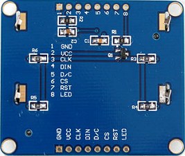
The device uses an inexpensive and commonly available graphical 84x48 LCD - the Nokia 5110. It comes mounted on a small breakout board with an 8-pin header but, unfortunately, I'm aware of at least three different pinout arrangements which makes designing a "universal" PCB difficult if not impossible.
 |  |  |
| ebay.co.uk/itm/180923746869 | ebay.co.uk/itm/230875451328 | adafruit.com/products/338 |
To simplify redesigning the PCB layout to suit different LCD breakout boards, I've connected every pin on the board, except GND, to an OUTPUT on the ATmega328.
Hopefully, the PCB should be adaptable with only minor changes. The 120R resistor for the LED is useful to act as a 'jumper' to the appropriate pin. It should be noted that some displays have the LED pin connected to 0v to light and others have it connected to Vcc. Luckily, by wiring the LED pin to an ATmega output, this is easily accomodated via the software and, by connecting the LED to a PWM-cabable output, the brightness can be adjusted in software.
The size of the Adafruit board is slightly different to the other two and probably would not fit alongside the navigation switch in the enclosure that I've used.
One consequence of connecting all the Nokia 5110 pins to the ATmega328 is that there aren't enough Digital pins so analog pins A0 to A4 are configured as digital OUTPUTS. In fact, A5 is the only analog input pin to escape unscathed!
Power Supply
The Nokia 5110 is a 3.3v device so some thought was given to the type of power supply.The ATmega328 will run happily at 3.3v so, rather than mess around with voltage level converters, it makes sense to run the whole circuit at 3.3v. This means that an external programmer connected to ATmega328 pins 1, 2 and 3 absolutely must NOT supply 5v to our circuit unless the Nokia 5110 display is removed and the internal battery disconnected. I've designed the PCB, so that what would be the 5v input to the programming header from the programmer is deliberately left unconnected.
Our project obviously has to be portable, ie battery powered, and the simplest option is to use a CR2032 button cell. The problem is these cells are only 3 volts (which is just about ok) but they quickly lose their initial voltage. I've designed a simple PCB to use with a CR2032 holder.
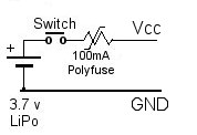
I've had no experience with rechargeable Lithium Polymer batteries but this project seemed a good opportunity to try one out - especially as small size was a major consideration for this project. I settled for this 110mAh battery which has internal circuitry to protect itself from reasonable abuse. Even so, despite the battery's in-built protection, I've also included a 100mA resettable fuse (polyfuse) in the circuit. Even a tiny 110mAh LiPo battery could deliver a LOT of current in the event of a fault somewhere in the project.
At 3.7 volts (nominal) it would probably be just about safe to connect it directly to the Nokia 5110 except the lithium polymer's fully charged voltage is 4.2 volts which I consider a bit too high for comfort. As a result, I've included a 3.3v very low drop-out regulator. It requires a 0.2 volt differential so should give a reasonable "range" of usable voltage from the LiPo.
When the Controller is operating in modes which don't require the photodiode to be "poised for action" continuously, I've arranged the software to put the ATmega328 in Power-Down mode which reduces the current consumption dramatically - from around 8mA down to about 1.5µA -- yes microamps! Unfortunately, one consequence of using the 3v3 regulator is that the regulator itself requires current, resulting in a Power-Down current of around 0.5mA. Obviously not as good but still a worthwhile saving.
It has been pointed out on the Arduino forum that the MCP1702-3302E/TO would be a better choice for the regulator because its standby (quiescent) current is only around 2uA. It would need a slight re-design of the power supply PCB because the regulator's pinout is different but I didn't get around to this.... see "Update"...
Update:

 The Nokia display that I bought is advertised as "VCC - power input (3.3v and 5v available)". After some deliberation, I
decided to run mine at 4.2 volts (the battery's fully charged voltage). It has run continuously for several days (on a mains
power supply) with no issues. I, therefore, decided to run mine permanently without the voltage regulator and designed a new
power supply PCB to suit. The advantages are that all of the battery voltage is available to the controller and, in PowerDown
mode, the total current drawn by the unit is less than 2µA.
The Nokia display that I bought is advertised as "VCC - power input (3.3v and 5v available)". After some deliberation, I
decided to run mine at 4.2 volts (the battery's fully charged voltage). It has run continuously for several days (on a mains
power supply) with no issues. I, therefore, decided to run mine permanently without the voltage regulator and designed a new
power supply PCB to suit. The advantages are that all of the battery voltage is available to the controller and, in PowerDown
mode, the total current drawn by the unit is less than 2µA.The simplified power supply circuit is shown here. The new power supply PCB layout is included on the next page as an option. Whether or not other displays will run safely on 4.2 volts is for you to decide.
In the next section, we look at the PCB layout....