The Printed Circuit Boards
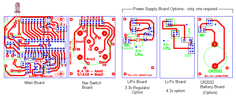
The photo above shows the main board and the Navigation Switch board near the end of construction. To get a snug fit, I filed the PCBs around any "obstructions" inside the enclosure. When finally assembled, the navigation switch fits into the top half of the case and will move about 1cm to the left from its position in this photo and fit snugly alongside the LCD display.
Although the PCB layout provides for header pins (or sockets) for the wires to the 7-way navigation switch, as I didn't have anything small enough available, I just soldered the wires directly to the PCB.
As I mentioned previously, there is potentially a high voltage at the flash (PC) connector so I used a short length of screened cable with a decent thickness outer sheath for the connection between the PC socket and the opto-isolator.
The ATmega328 programming socket is designed to be used with an external RS232-to-TTL converter such as the one shown here.
Download Circuit Wizard PCB Layout.
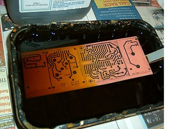 This photo shows the boards being etched.
The two small boards at extreme left and extreme right are for the power supply options. I wasn't sure at this stage which power supply option I'd be using so I etched both boards while I had the etching equipment out.
Note that some tracks on the main board are, of necessity, very close to the edge of the board and the thin border of copper around each board needs to be filed away once etching is complete and the boards have been separated.
|
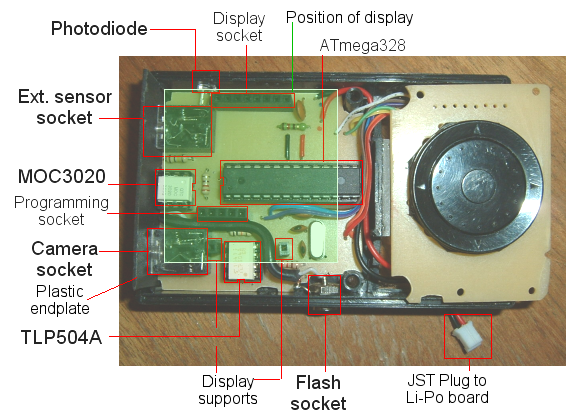
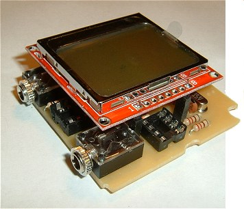
This photo (left) shows the main printed circuit board during construction, with the Nokia 5110
mounted on top. Note the two single-pin supports for the Nokia 5110 - one either side of the socket for the TLP505A opto-isolator. As an alternative, the display could be supported with a piece of foam stuck to the top of the ATmega328. The end plate supplied with the enclosure was too thick to allow the 3.5mm sockets' locknuts to fit so I made a new endplate from some black plastic sheet (a piece cut from an old DVD case!). The photo on the right shows the simplified (4.2v) power supply board. | 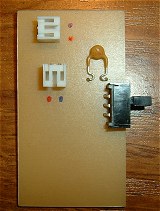 |
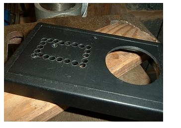 | The cutouts in the top half of the case were both made by chain-drilling
and filing. The Enclosure was from Farnell. The photo on the right shows the power supply PCB fitted in the enclosure's battery compartment. A piece of plastic sheet sits between this PCB and the back of the navigation switch PCB. | 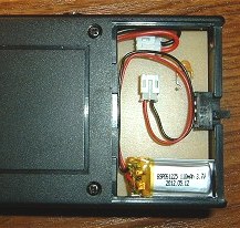 |